Hello.
I’m semiconductor engineer.
I want to mark on the wafer images. And I want to organize a node to determine how distorted the wafer is.
Can I use Knime?
Thank you ![]()
Hello.
I’m semiconductor engineer.
I want to mark on the wafer images. And I want to organize a node to determine how distorted the wafer is.
Can I use Knime?
Thank you ![]()
Yes you can.
Have a look here:
KNIME Image Processing | KNIME
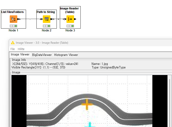
Hi @ActionAndi.
I can view the image through the Image Reader node.
However, the contents of the link do not seem to be able to mark the desired point in the image.
How should I configure the nodes?
Thank you.
Hi,
well I didn’t expect that the image processing nodes would solve your task right out of the box.
So you have to develop a strategy how to determine the distortion. I would start with something like this: